摘要:本文針對由FPGA構成的高速數據採集系統數據處理能力弱的問題,提出FPGA與單片機實現數據串列通信的解決方案。在通信過程中完全遵守RS232協議,具有較強的通用性和推廣價值。
1 前言
現場可編程邏輯器件(FPGA)在高速採集系統中的應用越來越廣,由於FPGA對採集到的數據的處理能力比較差,故需要將其採集到的數據送到其他CPU系統來實現數據的處理功能,這就使FPGA系統與其他CPU系統之間的數據通信提到日程上,得到人們的急切關注。本文介紹利用VHDL語言實現 FPGA與單片機的串口非同步通信電路。
整個設計採用模塊化的設計思想,可分為四個模塊:FPGA數據發送模塊,FPGA波特率發生控制模塊,FPGA總體介面模塊以及單片機數據接收模塊。本文著重對FPGA數據發送模塊實現進行說明。
2 FPGA數據發送模塊的設計
根據RS232 非同步串列通信來的幀格式,在FPGA發送模塊中採用的每一幀格式為:1位開始位+8位數據位+1位奇校驗位+1位停止位,波特率為2400。本系統設計的是將一個16位的數據封裝成高位幀和低位幀兩個幀進行發送,先發送低位幀,再發送高位幀,在傳輸數據時,加上文件頭和數據長度,文件頭用555555來表示,只有單片機收到555555時,才將下面傳輸的數據長度和數據位進行接收,並進行奇校驗位的檢驗,正確就對收到的數據進行存儲處理功能,數據長度可以根據需要任意改變。由設置的波特率可以算出分頻係數,具體演算法為分頻係數X=CLK/(BOUND*2)。可由此式算出所需的任意波特率。下面是實現上述功能的VHDL源程序。
Library ieee;
use ieee.std_logic_1164.all;
use ieee.std_logic_arith.all;
use ieee.std_logic_unsigned.all;
entity atel2_bin is
port( txclk: in std_logic; --2400Hz的波特率時鐘
reset: in std_logic; --複位信號
din: in std_logic_vector(15 downto 0); --發送的數據
start: in std_logic; --允許傳輸信號
sout: out std_logic --串列輸出埠
);
end atel2_bin;
architecture behav of atel2_bin is
signal thr,len: std_logic_vector(15 downto 0);
signal txcnt_r: std_logic_vector(2 downto 0);
signal sout1: std_logic;
signal cou: integer:=0;
signal oddb:std_logic;
type s is(start1,start2,shift1,shift2,odd1,odd2,stop1,stop2);
signal state:s:=start1;
begin
process(txclk)
begin
if rising_edge(txclk) then
if cou<3 then thr<="0000000001010101"; --發送的文件頭
elsif cou=3 then
thr<="0000000000000010"; --發送的文件長度
elsif (cou>3 and state=stop2) then thr<=din;--發送的數據
end if;
end if;
end process;
process(reset,txclk)
variable tsr,tsr1,oddb1,oddb2: std_logic_vector(7 downto 0);
begin
if reset='1' then
txcnt_r<=(others=>'0');
sout1<='1';
state<=start1;
cou<=0;
elsif txclk'event and txclk='1' then
case state is
when start1=>
if start='1' then
if cou=3 then
len<=thr;
end if;
tsr:=thr(7 downto 0);
oddb1:=thr(7 downto 0);
sout1<='0'; --起始位
txcnt_r<=(others=>'0');
state<=shift1;
else
state<=start1;
end if;
when shift1=>
oddb<=oddb1(7) xor oddb1(6) xor oddb1(5) xor oddb1(4) xor oddb1(3) xor oddb1(2) xor oddb1(1) xor oddb1(0);
sout1<=tsr(0); --數據位
tsr(6 downto 0):=tsr(7 downto 1);
tsr(7):='0';
txcnt_r<=txcnt_r+1;
if (txcnt_r=7) then
state<=odd1;cou<=cou+1;
end if;
when odd1=> --奇校驗位
if oddb='1' then
sout1<='0';state<=stop1;
else
sout1<='1';state<=stop1;
end if;
when stop1=>
sout1<='1'; --停止位
if cou<4 then
state<=start1;
else
state<=start2;
end if;
when start2=>
tsr1:=thr(15 downto 8);
oddb2:=thr(15 downto 8);
sout1<='0'; --起始位
txcnt_r<=(others=>'0');
state<=shift2;
when shift2=>
oddb<=oddb2(7) xor oddb2(6) xor oddb2(5) xor oddb2(4) xor oddb2(3) xor oddb2(2) xor oddb2(1) xor oddb2(0);
sout1<=tsr1(0);--數據位
tsr1(6 downto 0):=tsr1(7 downto 1);
tsr1(7):='0';
txcnt_r<=txcnt_r+1;
if (txcnt_r=7) then
state<=odd2;
end if;
when odd2=> --奇校驗位
if oddb='1' then
sout1<='0';state<=stop2;
else
sout1<='1';state<=stop2;
end if;
when stop2=>
sout1<='1'; --停止位
if len="0000000000000000" then
state<=stop2;
else
state<=start1;
len<=len-1;
end if;
end case;
end if;
end process;
sout<=sout1;
end behav;
其中各信號的說明已在程序中標明了。波形模擬圖如圖2所示。
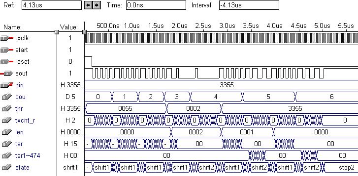
圖2 FPGA數據發送時序模擬圖
圖中Din寫入值為3355H,波特率為2400Hz,Start信號始終置邏輯1,即隨時都能發送數據。Reset信號邏輯1時複位,邏輯0時電路開始工作。THR是數據寄存器,文件頭、數據長度以及數據位都先寄存到THR中,Len是數據長度,TSR是低8位數據幀寄存器,TSR1是高8位數據幀寄存器。數據長度Len定為02H,發送時先發送低8位55H,后發送高8位33H,一共發送兩遍。發送的數據格式說明:當發送55H時,其二進位為01010101,則發送的數據的二進位數為00101010111(1位開始位+8位數據位+1位奇校驗位+1位停止位)。
單片機部分先對FPGA發送過來的文件頭進行確認,正確就接收文件,否則放棄接收的數據。根據FPGA發送模塊的協議,對串口控制寄存器SCON和波特率控制寄存器PCON的設置即可實現。
3 總結
目前電子產品的開發中經常要綜合運用EDA技術、計算機控制技術、數字信號處理技術,那麼電路各部分經常需要數據交換。本文也是基於此給出這方面應用的實例,供開發者交流。
參考文獻
[1] 潘松,黃繼業著.EDA技術實用教程[M].北京:科學出版社,2002.
[2] 林敏,方穎立著.VHDL數字系統設計與高層次綜合[M].北京:電子工業出版社,2002.
[3] 王振紅著.VHDL數字電路設計與應用實踐教程[M].北京:機械工業出版社,2003.
[4] 徐維祥,劉旭敏著.單片微型機原理及應用[M].大連:大連理工大學出版社,2002.
[admin via 研發互助社區 ] FPGA和單片機串列通信介面的實現已經有3492次圍觀
http://cocdig.com/docs/show-post-42953.html
