Powerint LNK605DG高效3.6W LED驅動方案
Powerint公司的LinkSwitch-II系列 LNK605DG集成了700V功率MOSFET,新穎的OM/OFF控制狀態機,用於自偏壓的高壓開關電流源,逐個周期的電流限制以及延遲的熱關斷電路。由於不需要光耦合器和次級控制電路,因此大大地簡化了低功率CV/CC充電器的設計。230VAC時無負載的功耗低於30mW,主要用於手機/無繩電話,PDA,MP3/手提音頻設備的充電器,以及LED驅動器等。本文介紹了LinkSwitch-II系列 LNK605DG主要特性,功能方框圖,高能效USB充電器電路圖,無偏壓電源的反激電源電路圖以及採用LinkSwitchTM-II LNK605DG的高效(≥75%) 3.6W絕緣led驅動器參考設計主編要特性與指標,電路圖和材料清單(BOM)。
The LinkSwitch-II dramatically simplifies low power CV/CC charger designs by ELiminating an optocoupler and secondary control circuitry. The device introduces a revolutionary control technique to provide very tight output voltage and current regulation, compensating for transformer and internal parameter tolerances along with input voltage variations.
The device incorporates a 700 V power MOSFET, a novel ON/OFF control state machine, a high voltage switched current source for self biasing, frequency jittering, cycle-by-cycle current limit and hysteretic thermal shutdown circuitry onto a monolithic IC.
LNK605DG 產品亮點:
Dramatically Simplifies CV/CC Converters
? Eliminates optocoupler and all secondary CV/CC control circuitry
? Eliminates all control loop compensation circuitry
Advanced Performance Features
? Compensates for transformer inductance tolerances
? Compensates for input line voltage variations
? Compensates for cable voltage drop (LNK61X series)
? Compensates for external component temperature variations
? Very tight IC parameter tolerances using proprietary trimming technology
? Frequency jittering greatly reduces EMI filter cost
? Even tighter output tolerances achievable with external resistor selection/trimming
? Programmable switching frequency up to 85 kHz to reduce transformer size
Advanced Protection/Safety Features
? Auto-restart protection reduces power delivered by >95% for output short circuit and control loop faults (open and shorted components)
? Hysteretic thermal shutdown – automatic recovery reduces power supply returns from the field
? Meets high voltage creepage requirements between DRAIN and all other pins both on the PCB and at the package
EcoSmart® – Energy Efficient
? Easily meets all global energy efficiency regulations
? No-load consumption below 30 mW at 230 VAC with optional external bias winding
? ON/OFF control provides constant efficiency down to very light loads – ideal for CEC and ENERGY STAR 2.0 regulations
? No current sense resistors – maximizes efficiency
Green Package
? Halogen free and RoHS compliant package
LNK605DG 應用:
? Chargers for cell/cordless phones, PDAs, MP3/portable audio devices, adapters, LED drivers, etc.
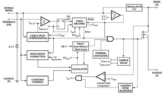
圖1。LNK605DG功能方框圖
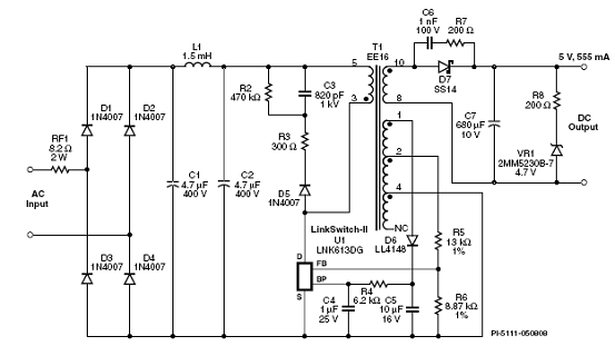
圖2。LNK605DG高能效USB充電器電路圖(平均效率74%,無負載輸入功率小於30mW)
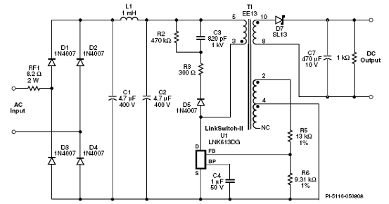
圖2。無偏壓電源的LinkSwitch-II 反激電源電路圖
採用LinkSwitchTM-II LNK605DG的高效(≥75%) 3.6W絕緣LED驅動器參考設計
The document describes a high efficiency LED driver designed to drive 12 V at 0.3 A from an input voltage range of 90 VAC to 265 VAC. The LED driver uses the LNK605DG from the LinkSwitch-II family by Power Integrations.
LinkSwitch-II ICs allow the implementation of cost effective and low component count LED drivers meeting the compact design and high efficiency requirements necessary for high temperature operating environments.
The topology used is an isolated flyback operating in discontinuous conduction mode. Output current regulation is sensed entirely from the primary side eliminating the need for secondary side feedback components. No external current sensing is required on the primary side either as this is performed inside the IC further reducing components and losses.
The LNK605DG also provides a sophisticated range of protection features including autorestart for open control loop and output short-circuit conditions. Accurate hysteretic thermal shutdown ensures safe average PCB temperatures under all conditions. In LED luminaires the driver determines many of the performance attributes experienced by the end user including startup time and unit to unit consistency. For this design, the LNK605DG device ensures unit to unit consistency with an output CC tolerance of <?10%, fast startup time of <5 ms for instant on performance and long lifetime and high reliability due to the low component count.
This document contains the LED driver specification, schematic, PCB diagram, bill of materials, transformer documentation and typical performance characteristics.
3.6W絕緣LED驅動器參考設計主要特性:
?
Low cost, low component count and small printed circuit board footprint solution
Frequency jitter for smaller, lower cost EMI filter components
Primary side control eliminates secondary side control and optocoupler and provides +/-5% CV and +/-10% CC accuracy
?
Integrated protection and reliability features
Output open circuit / output short-circuit protected with auto-recovery
Over-temperature protection – tight tolerance (+/-5%) with hysteretic recovery for safe PCB temperature under all conditions
Extended package pin creepage distance for reliable operation in humid environments - >3.2mm at package Designed to meet
EN55015B conducted EMI with >10 dBμV margin
IEC61000-4-5 Class 3 AC line surge
IEC61000-4-2 ESD at 4 kV contact / 8 kV air.
Ultra-low AC leakage current: <5 μA at 265 VAC input (no Y capacitor required) EcoSmartTM
No-load consumption: <50 mW at 265 VAC
Efficiency: ≥75% at both 115 VAC and 230 VAC
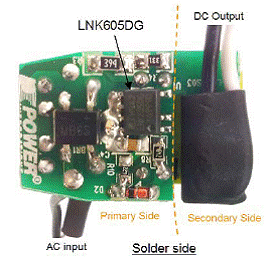
圖3。3.6W絕緣LED驅動器參考設計外形圖
3.6W絕緣LED驅動器電源指標:
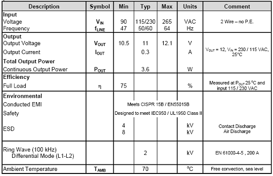
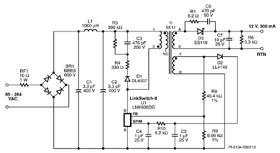
圖4。3.6W絕緣LED驅動器參考設計電路圖
3.6W絕緣LED驅動器參考設計材料清單(BOM):
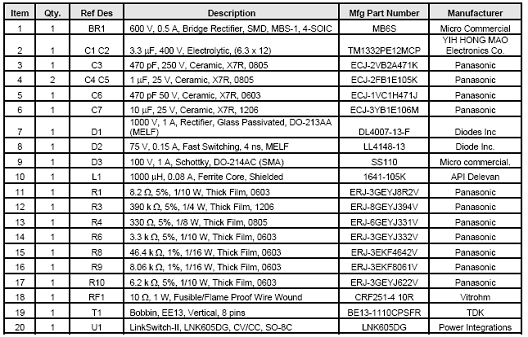
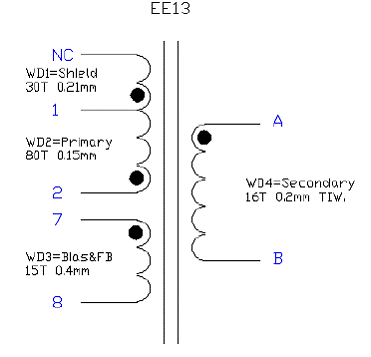
圖5。變壓器電路圖
